PCB Design for ESP32 Automation of 30A relays
Designing a 30A ESP32 Home Automation Circuit using KiCAD 🏠
OVERVIEW:
The goal was to create a safe, reliable, and high-current circuit for IoT-based home automation. Along the way, I learned not just about schematic capture and PCB design, but also about practical layout techniques that matter when handling significant current.
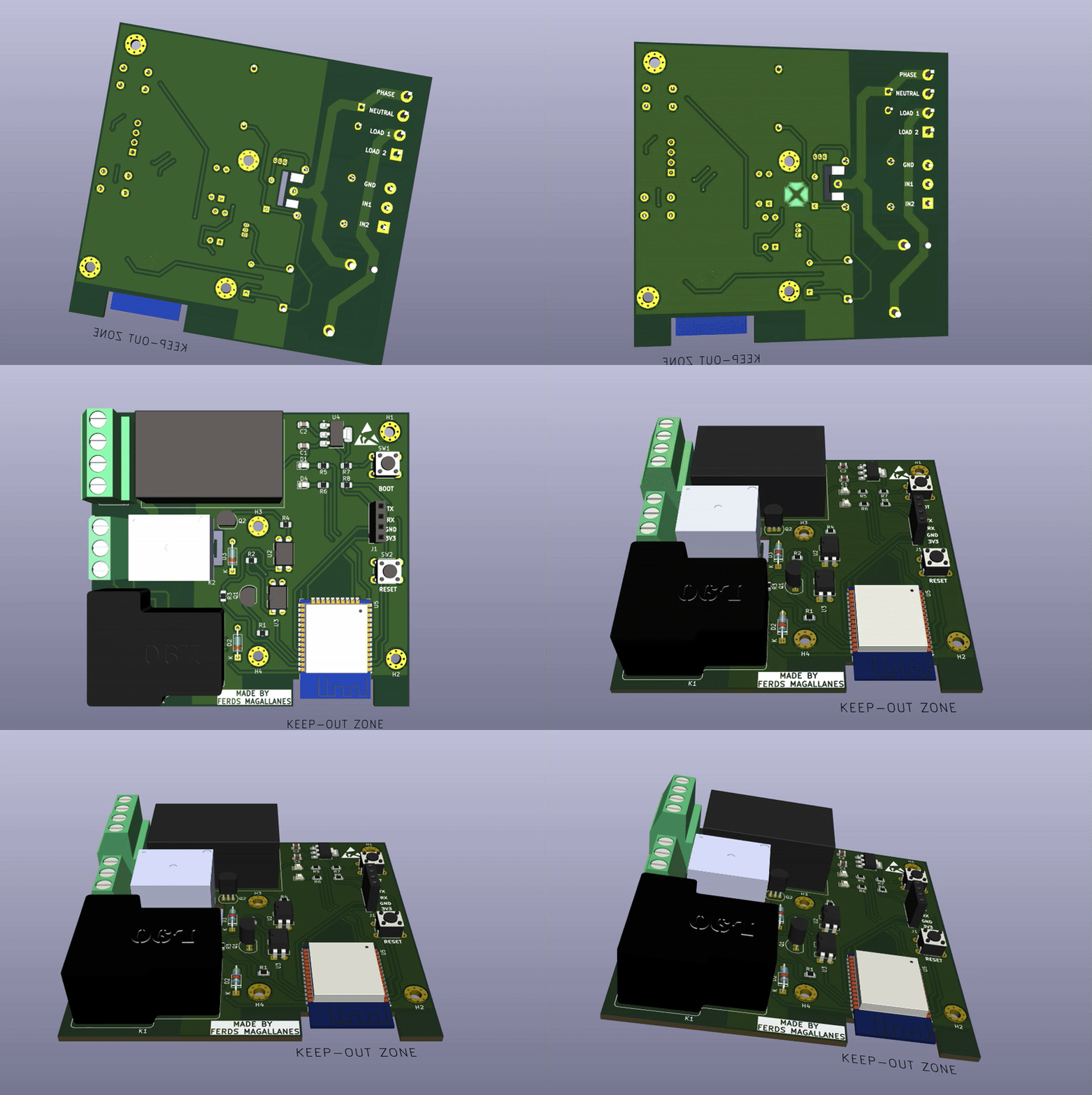
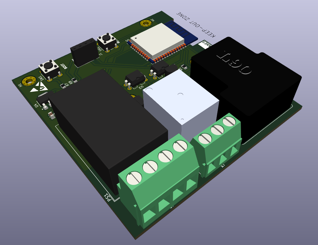
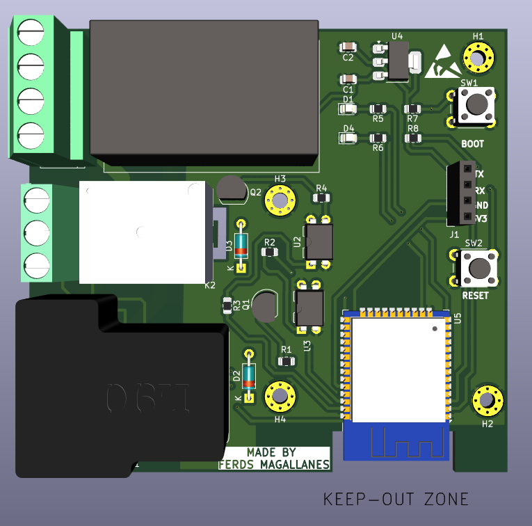
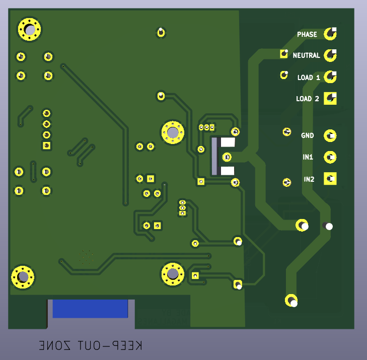
FINDINGS:
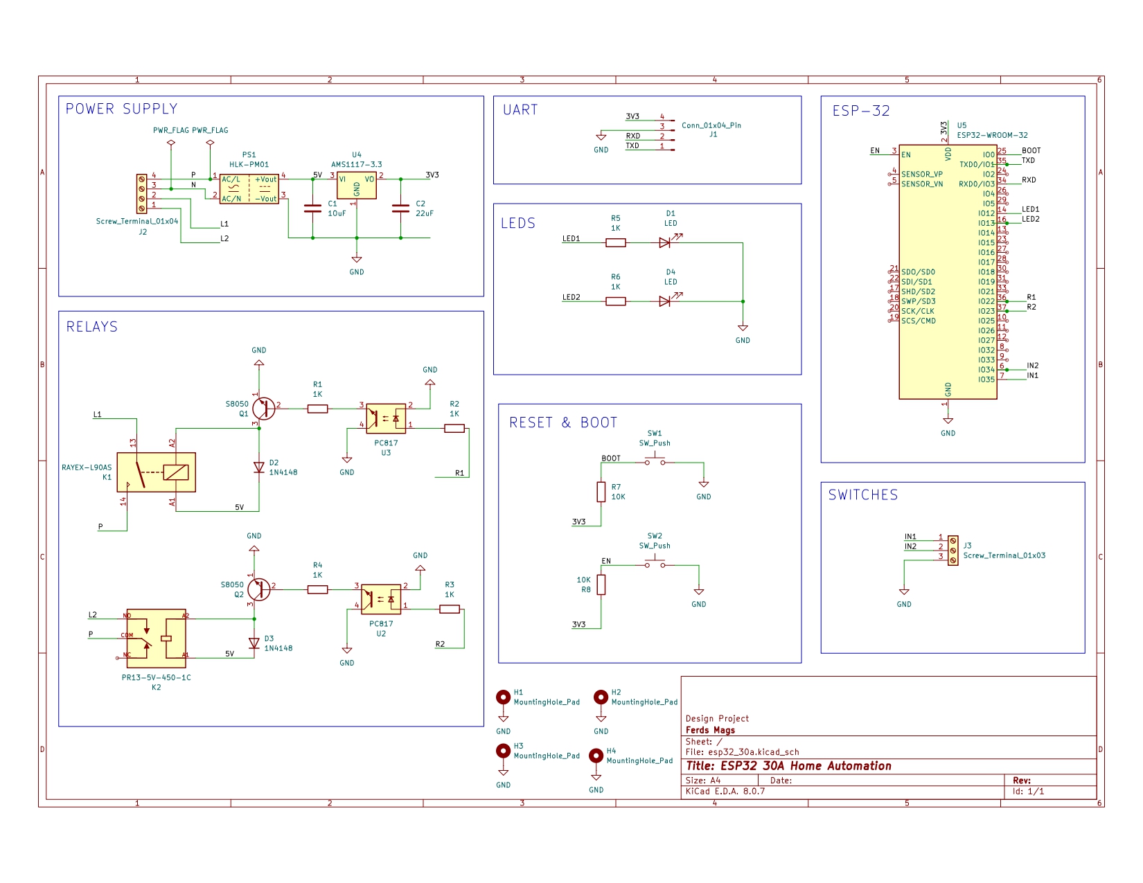
With the advent of IoT, there is a market for the control of multiple electrical items at home. This project is made with that intention in mind. ESP32 is the central microcontroller with Wi-Fi/ Bluetooth connectivity ideal these types of applications. It will govern the needed current to flick the relay poles from chosen relay/octocoupler components. In detail, the following analog/digital components are highlighted the functionality and safety of the board made:
- Relays (K1:
RAYEX-L90AS, K2:PR13-5V-450-1C)- These handle 30A / mains-level switching, isolating high voltage from the low-voltage ESP32 domain.
- Optocouplers (U2, U3:
PC817)- Provide
electrical isolationbetweenESP32 GPIO signalsandrelay driver circuits. - Prevents voltage spikes or surges on the relay side from damaging the ESP32.
- Critical safety feature separating low-voltage control logic (ESP32) from high-voltage relay switching.
- Provide
- Transistors (Q1, Q2:
S8050 NPN BJTs)- Act as
drivers to energize the relay coils, since ESP32 GPIO pins cannot supply enough current directly.
- Act as
- Flyback Protection with Diodes (D2, D3: 1N4148)
- Likely used as
flyback diodesacross relay coils. - Protects
transistors and ESP32 from voltage spikescaused by coil inductance when the relay is turned off.
- Likely used as
- Status Indication with LEDs (D1, D4)
- Provide visual feedback when relays or control signals are active.
- Stable Power Regulation
- AMS1117-3.3 (U4) → provides a regulated 3.3V supply for ESP32.
- HLK-PM01 (PS1) → an isolated AC-DC converter (230V AC → 5V DC), ensures compact, safe, and isolated power supply for the whole system.
- Push Buttons (SW1, SW2)
-
Allow manual override or testing of the circuit, which is also important in safety-critical systems.
-
LEARNINGS:
This project comes with its own setbacks and deviation from the schematic source in which I was basing it from, hence, I’m proud that with my own tracing and decisions created this unique PCB design. The learnings that I was able to get from this project is the following:
Using Vias Effectively
- Vias are critical when routing signals between PCB layers.
- For high-current traces, multiple vias in parallel reduce resistance and improve thermal performance.
- This reinforced the idea that vias aren’t just “signal tunnels” — they’re part of the current-carrying capacity of the design.
Copper Zones & Ground Planes
- I applied copper pour zones to handle higher current paths and improve grounding.
- I was able to tackle electrical signal discharge (ESDs) using this feature as it minimizes voltage drops and reduces EMI in sensitive circuits.
- It also makes soldering easier since larger copper areas can help with thermal dissipation.
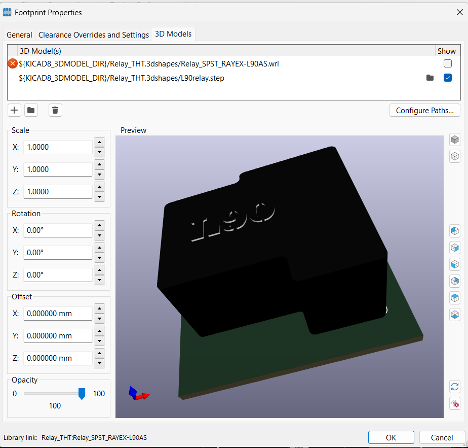
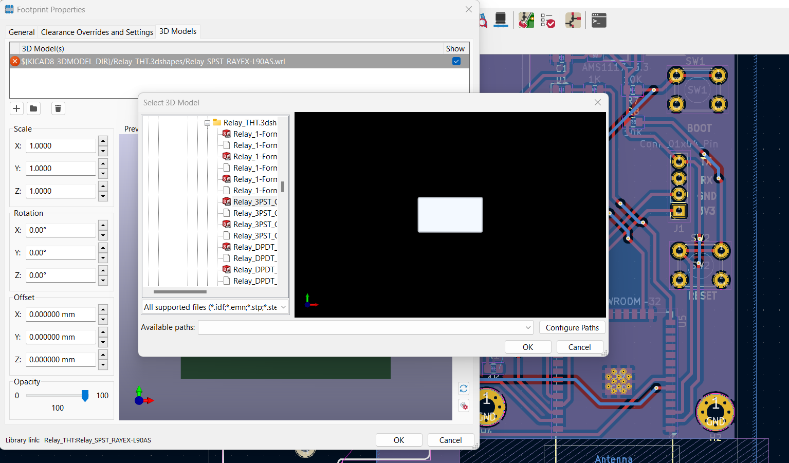
_Replacing & Updating CAD Components | Troubleshooting
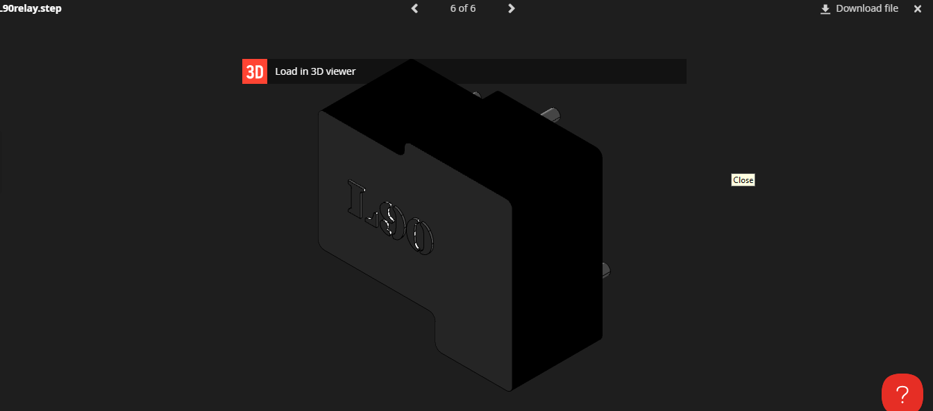
- Some of the initial footprints and 3D models were missing or broken.
- I learned to replace them with updated library components and assign correct 3D models.
- This improved not just the functional accuracy of the PCB but also gave me a realistic 3D preview of the board — crucial for verifying clearances in enclosures. Kindly check the images below pertaining to this!!
Overall, I was able to do the following:
Schematic Capture
- Placed the ESP32, relays, connectors, and supporting components.
- Double-checked footprints for high-current parts.
PCB Layout
- Oriented relays and connectors to streamline wiring.
- Added wide copper traces and copper zones to support 30A current flow.
- Used vias strategically to distribute current across layers. I may have made some inefficiencies in the routing using this method but overall, the PCB design should be functional
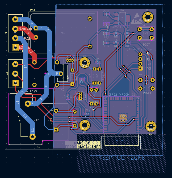
- Final Checks
- Ran Design Rule Check (DRC) to catch clearance issues.
- Updated missing 3D models for realistic visualization.
- Viewed the completed design in the 3D viewer to ensure correct placement and alignment.
This was fun for me since I got to experiment with ESP32 for PCB use and specific functions :>
PS. Whats left of this design is to acutally test it with the physical components but overall, with the checks that I did, it should be ready for production as I also did consider it for manufacturing! EDA and CAD is available upon request.