PCB Design for Traffic Light Sim
a simple printed circuit board design (PCB) for a traffic light indicator 🚦
OVERVIEW:
The objective of the project is to make a simple PCB to be used for simulating a traffic light indicator that can be controlled via a microcontroller. This is to get my feet wet on PCB design!!

FINDINGS:
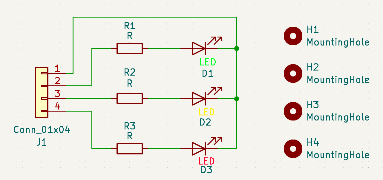
I was able to do schematic capture and component management as well as PCB layout and routing. Particularly, I was able to do the following:
Schematic Capture & Component Management
-
Symbol Insertion & Library Use- KiCad allows you to browse and import components from its symbol libraries directly into my schematic
- You can
swap or updatesymbols easily using tools like “Change Symbol…” or “Update Symbol from Library…” to keep my design aligned with the latest library versions
- Connecting Components
- Use
wires, buses, net labels, junctions, and power symbolsto clearly define electronic connections - Power symbols such as VCC or GND provide global net connections without requiring physical pins.
- Use
- Error Checking
- The
Electrical Rules Check (ERC)helps catch common wiring errors, floating pins, and missing values before transferring the design to PCB layout
- The


Generating PCB Layout from Schematic
- Component Placement
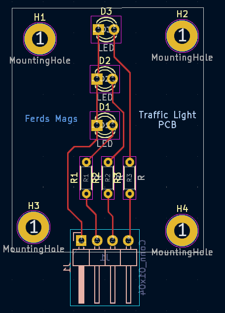
- Organize components in the PCB editor for clearer routing, mirroring my schematic to reduce wire crossings
- Routing Tracks
- Replace
air-wires with copper tracksusing the routing tool (X) and work with layers (F.Cu, B.Cu) for front/back trace layouts
- Replace
- Board Edge & Outline
-
Define my
board outlinewith an Edge. Cuts polygon to specify the physical shape of the PCB - Design Rule Check (DRC)
- Run DRC to catch
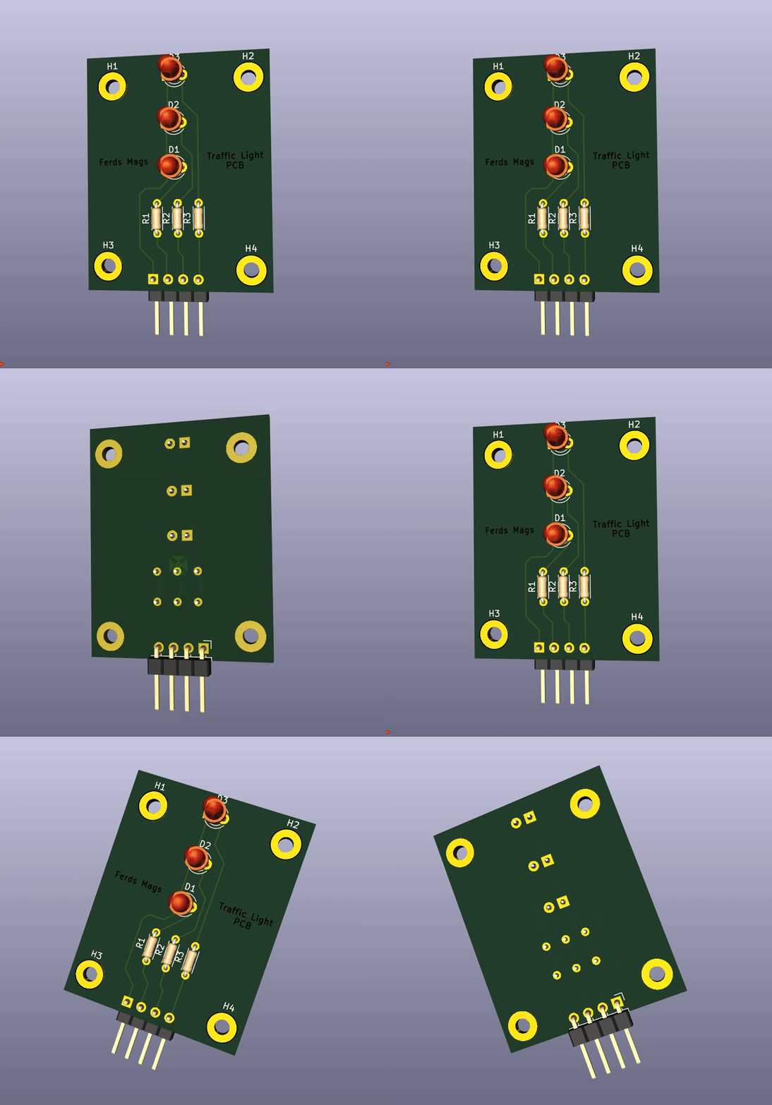
spacing violations,unconnected nets, andrule inconsistenciesbefore manufacturing - Visualize the finished board with components and copper features in a 3D viewer — a great way to catch mechanical placement issues
- Run DRC to catch

LEARNINGS
It was a rudimentary implementation of what I wanted but considering that I had no formal background in designing, I was quite proud of what I made and this will definitely be my starting point for more bigger projects in the future! KiCAD is my main choice of PCB design since it is free but I’ve been meaning to try also JLCPCB online as it directly makes the schematic and gives the rough BOM prices per component and it is ready to build on the given Gerber files. That is something I can improve one and will definitely try in my next PCB designing sesh!