PCB Design for a USB-C Type Charger for Powerbank
use of the MCP73811 and PAM2401 IC chips to make a USB-C type charger connected to a battery pack under Altium Designer
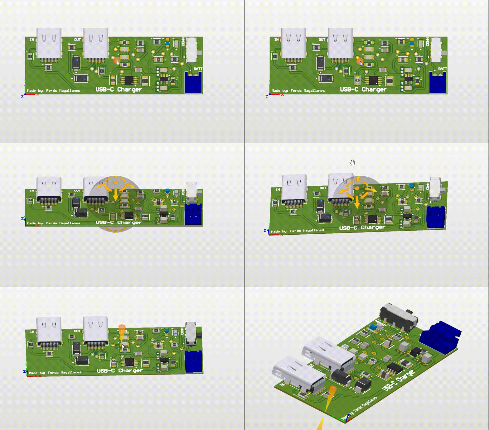
About the Thumbnail: This is the 3D model of the made USB Type-C charger typically seen in powerbanks to first provide in the in port a means to charge the connected battery and the out power to retrieve the stored power from rechargeable battery.
OVERVIEW:
This project focuses on designing and fabricating a compact USB Type-C charger capable of charging a single-cell Li-ion battery and providing a stable 5V output. The design integrates two primary ICs:
- MCP73811 — a linear Li-Ion/Li-Polymer battery charging controller from Microchip.
- PAM2401 — a step-up DC-DC converter from Diodes Inc., used to boost the 3.7V battery voltage to 5V.
The goal of this project was to create a cost-effective and manufacturable PCB charger with standard USB-C input/output and efficient power conversion. All circuit development was done in Altium Designer, including schematic capture, PCB layout, and CAM file generation for production.
Below is an explanation video for the project that details the execution of the project post-hoc!
METHODOLOGY:
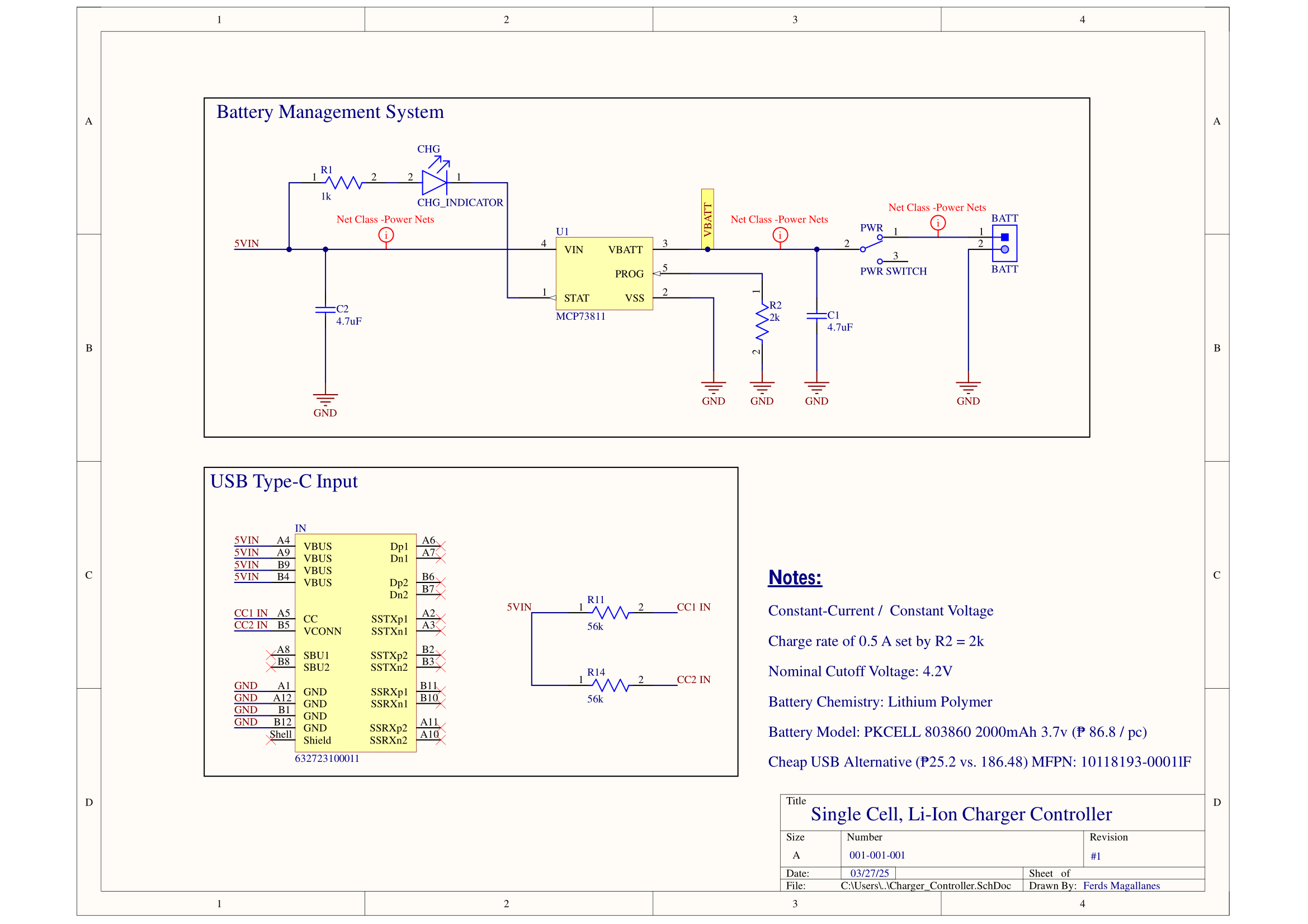
MCP73811 Battery Management System Based on the Microchip MCP73811 datasheet, the design implements a constant-current/constant-voltage charging profile suitable for 3.7V single-cell Li-ion batteries.
Key design parameters included:
- Charge current set to 0.5A using a 2kΩ resistor on the PROG pin.
- Cutoff voltage fixed at 4.2V, consistent with Li-ion chemistry.
- Input from the USB Type-C port is regulated through filtering capacitors (C1, C2) before feeding the MCP73811’s VIN pin.
- CHG indicator LED is connected to the STAT pin to display charge activity.
- A slide switch (JS102011JAQN) provides input power control.
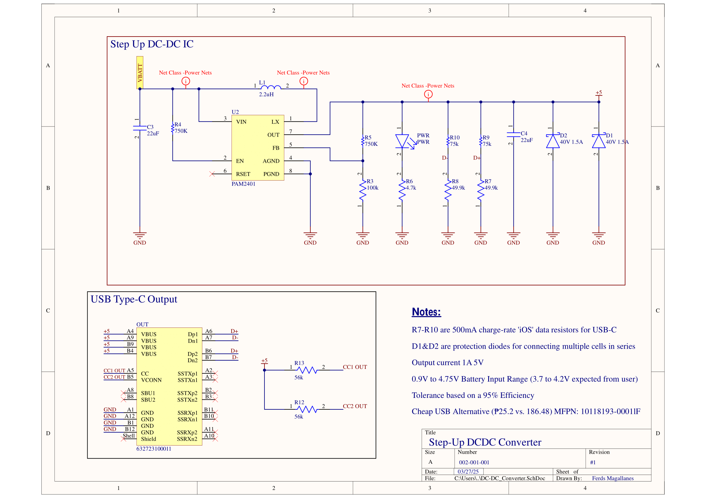
PAM2401 Step-Up Converter The PAM2401 is a 1.0MHz, high-efficiency boost converter that steps up the battery voltage (3.0–4.2V) to a regulated 5V USB output.
From the PAM2401 datasheet, the feedback network (R3–R6) and compensation capacitors (C3, C4) were designed to achieve:
- Output current up to 1A
- Input range from 0.9V to 4.75V
- Efficiency of approximately 95% under nominal load.
Schottky diodes (VS-15MQ040NTRPBF) and a 2.2µH inductor (TDK MLP2520S2R2MT0S1) handle power switching and energy storage, respectively. Output decoupling uses low-ESR capacitors for ripple suppression. Data resistors (R7–R10) were added to emulate USB iOS charge profiles on D+ and D– lines.
Kindly check further the manufacturing parts and materials considered for this project below.
LEARNINGS:
One of the conveniences of utilizing ALtium Designer is that I can immediately make a bill of materials from the manufacturers part search. This saves me a lot of time and definitely a neat feature to have when make such projects that often needs to have fast iterations per prototype.
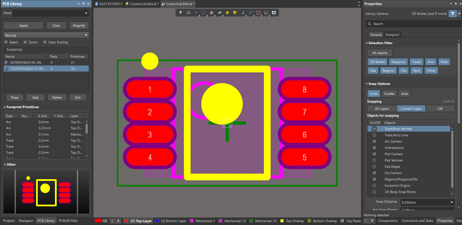
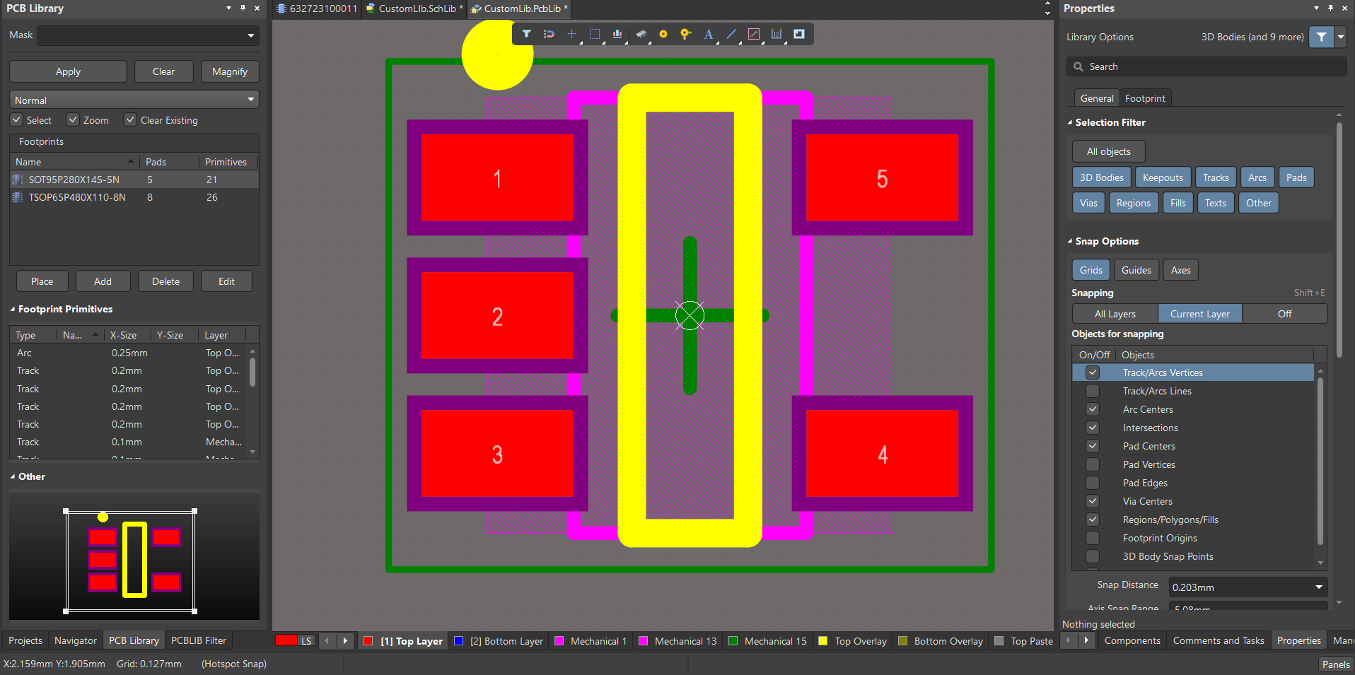
Another unique take that I was able to do for project is to make custom schematic diagrams for the IC chips in question for the project. Since the manufacturer of these chips does not provide the schematic footprint and the 3D models, I got the oppurtunity to make it own utilizing the in-built library and standards that the datasheets provided using the IPC Compliant footprint wizard from the tool tab of Altium using the small outline packages (SOP) convention. You may check my work on the images below.
Lastly, I have made the gerber files for sending to PCBway for them to check if it is ok for manufacturing. Considered Gerber and drill files directly through Altium’s CAM processor. Verified design rules (clearances, hole sizes) for manufacturability. Also considered a local PCB manufacturing which is DOST-ASTI! Exported a stack-up report summarizing copper, dielectric, and net connectivity layers.
HOW THIS PROJECT CAN BE FURTHER IMPROVED:
PCB layout can be further improved of course with better tracing and minimize size constraints. I was not able to consider short power loops for the PAM2401 boost converter to reduce noise. but I did have thicker and wider copper traces for BMS for current handling. Should this be considered for mass production, it is a need to include silkscreen labels for USB Type-C orientation and corresponding test points, which I did not consider since this will be mainly utilized for my other personal projects!